PCB Laser Cutting and Marking: You should know
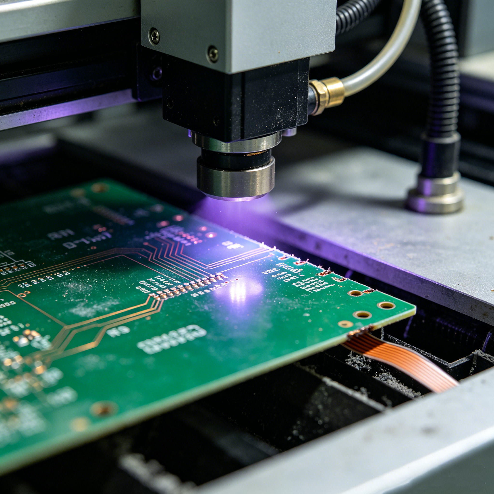
Printed circuit boards (PCBs) are the backbone of every electronic device. Cutting and marking them requires extreme precision. Mechanical routers can cause fraying, stress, and dust. That’s where PCB laser cutting and marking comes in. Lasers deliver clean edges, tiny feature sizes, and permanent markings without touching the board. Here’s everything you need to know.
1. What Is PCB Laser Cutting and Marking?
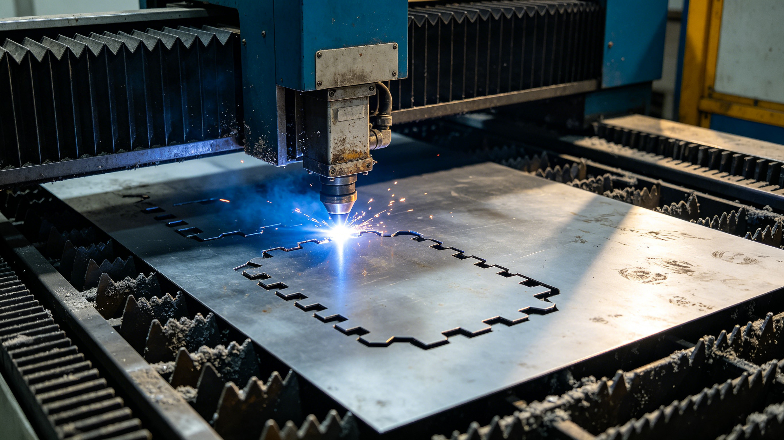
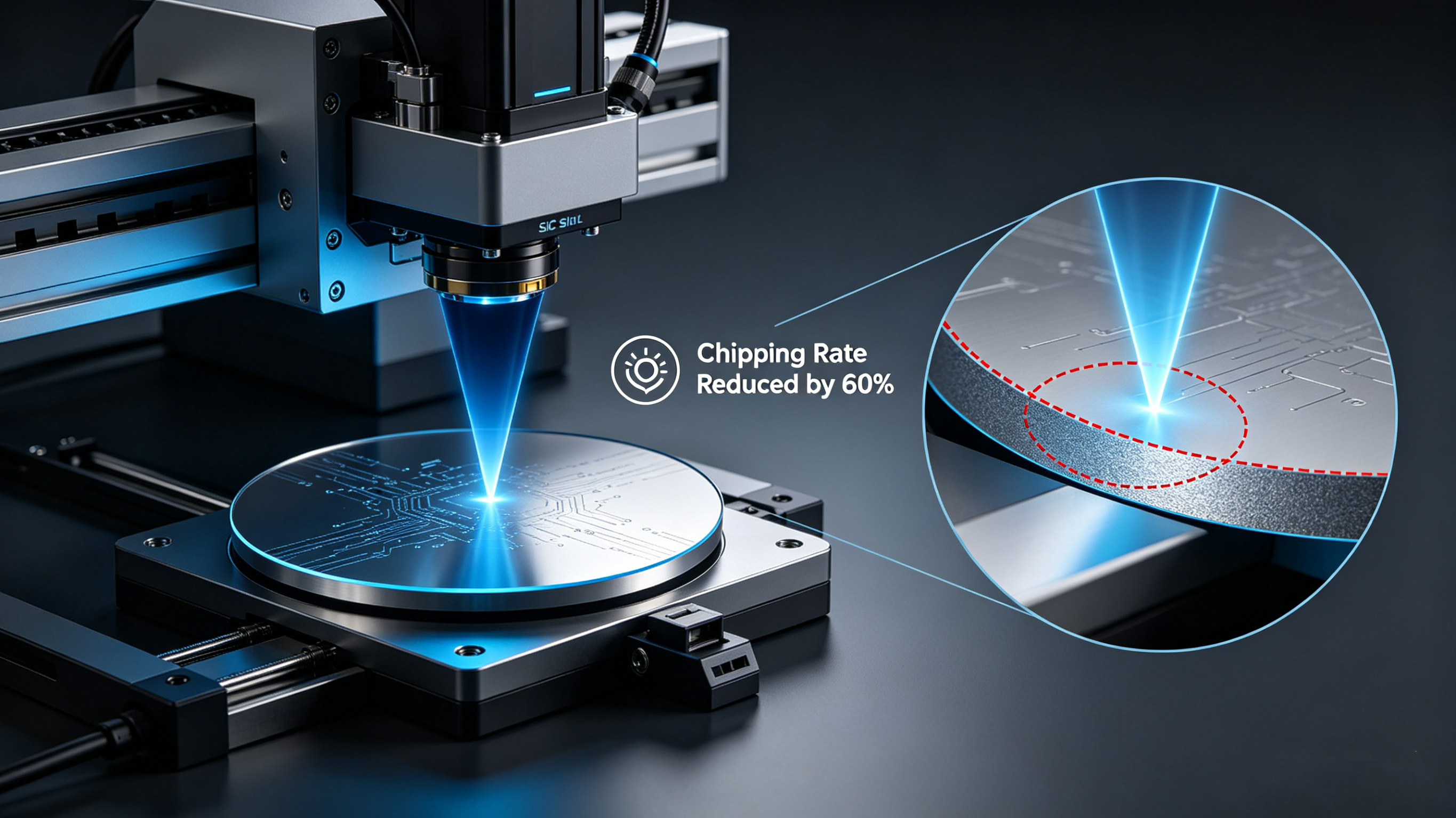
PCB laser cutting and marking refers to using a focused laser beam to cut through PCB materials (like FR4, copper, or flexible polyimide) and to engrave text, barcodes, or serial numbers onto the surface. It’s a non‑contact process. There are no cutting bits to wear out, and no mechanical stress on delicate traces. UV lasers are especially popular because their short wavelength is absorbed well by organics and metals, reducing heat damage.
2. How It Works (6 Steps)
-
PCB material preparation – The board is cleaned and fixed on the worktable.
-
CAD design import – Gerber or DXF files define cut paths and marking positions.
-
Calibration and setup – The laser system aligns to fiducial marks on the PCB.
-
Laser beam positioning – Galvanometer mirrors steer the beam at high speed.
-
PCB laser cutting – The laser vaporizes material along the programmed contour.
-
Additional finishing – Some systems also clean or deburr edges with a second pass.
3. Why Choose PCB Laser Cutting and Marking?
Five reasons manufacturers prefer it over traditional methods:
-
No mechanical stress – Delicate thin boards won’t crack or delaminate.
-
Ultra‑fine features – Cut lines as narrow as 0.1 mm, marks readable under a microscope.
-
No tool wear – A laser beam never gets dull, ensuring consistent quality.
-
Hole drilling in one step – Lasers can cut through and create micro‑vias simultaneously.
-
Clean process – Minimal dust, easily extracted.
4. Wide Applications of PCB Laser Cutting
PCB laser cutting and marking serves many segments:
-
PCB panelization – Separating individual boards from a production panel without burrs.
-
Solder paste stencils – Cutting precise apertures in stainless steel foil.
-
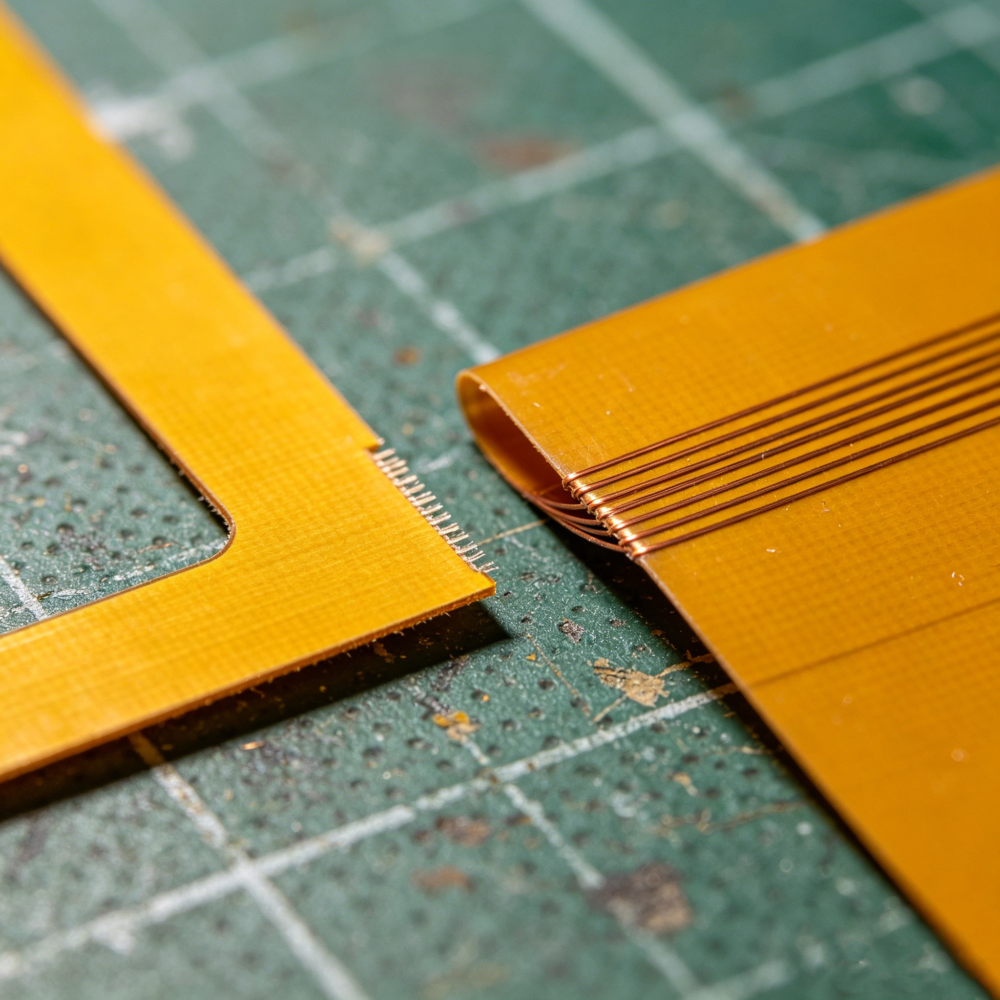
Flexible printed circuits – Laser cuts polyimide (Kapton) cleanly without frayed edges.
-
RF/microwave PCBs – Maintaining tight tolerances on high‑frequency materials.
-
LED PCBs – Marking component outlines and polarity symbols on metal‑core boards.
Each application benefits from the non‑contact, high‑precision nature of PCB laser cutting and marking.
5. How to Choose the Right Machine
Consider these four factors:
-
Technical specifications – Laser wavelength (UV for fine work, CO₂ for thicker organics), power, and spot size.
-
Brand reputation & reviews – Look for proven track records in electronics manufacturing.
-
Priority of needs – Do you need high speed, low cost, or ultra‑fine detail? Rank them.
-
Cost vs. efficiency – A cheaper machine may have higher operating costs or slower throughput.
Always ask for sample processing on your actual PCB before purchasing.
6. FAQ (Frequently Asked Questions)
Q1: Is PCB laser cutting more expensive than CNC routing?
A: The machine itself often has a higher upfront cost, but laser cuts faster, produces no tool wear, and eliminates deburring. For high‑volume or fine‑pitch boards, total cost per part is often lower.
Q2: Will the laser beam damage nearby components?
A: With proper beam alignment and shielding, no. UV lasers have very shallow heat‑affected zones, and modern systems use vision to avoid populated areas.
Q3: How fast is PCB laser cutting?
A: A 20W UV laser can cut through 1.6mm FR4 at about 10‑15 mm/s. Marking a 2D barcode takes less than one second. Speed varies with material and thickness.
Q4: Can it cut both rigid and flexible PCBs?
A: Yes. The same machine can handle FR4, CEM, polyimide, and even some metal‑core boards by adjusting power and speed.
Q5: What about safety and fumes?
A: Lasers are fully enclosed during operation. Built‑in HEPA and carbon filters remove smoke and odors. Operators must wear laser safety glasses.
Q6: Do I need special software?
A: Most machines work with standard EDA outputs (Gerber, DXF) via proprietary or third‑party laser software. Some offer direct import from popular design tools.
7. Final Thoughts
Adopting PCB laser cutting and marking improves yield, enables smaller designs, and reduces rework. Whether you prototype in a lab or run a high‑mix production line, this technology pays for itself quickly.
Ready to upgrade your PCB depaneling and marking process? Contact ZGLC Laser for a free sample test.
What You Should Know About CNC Machining: A Beginner’s Guide
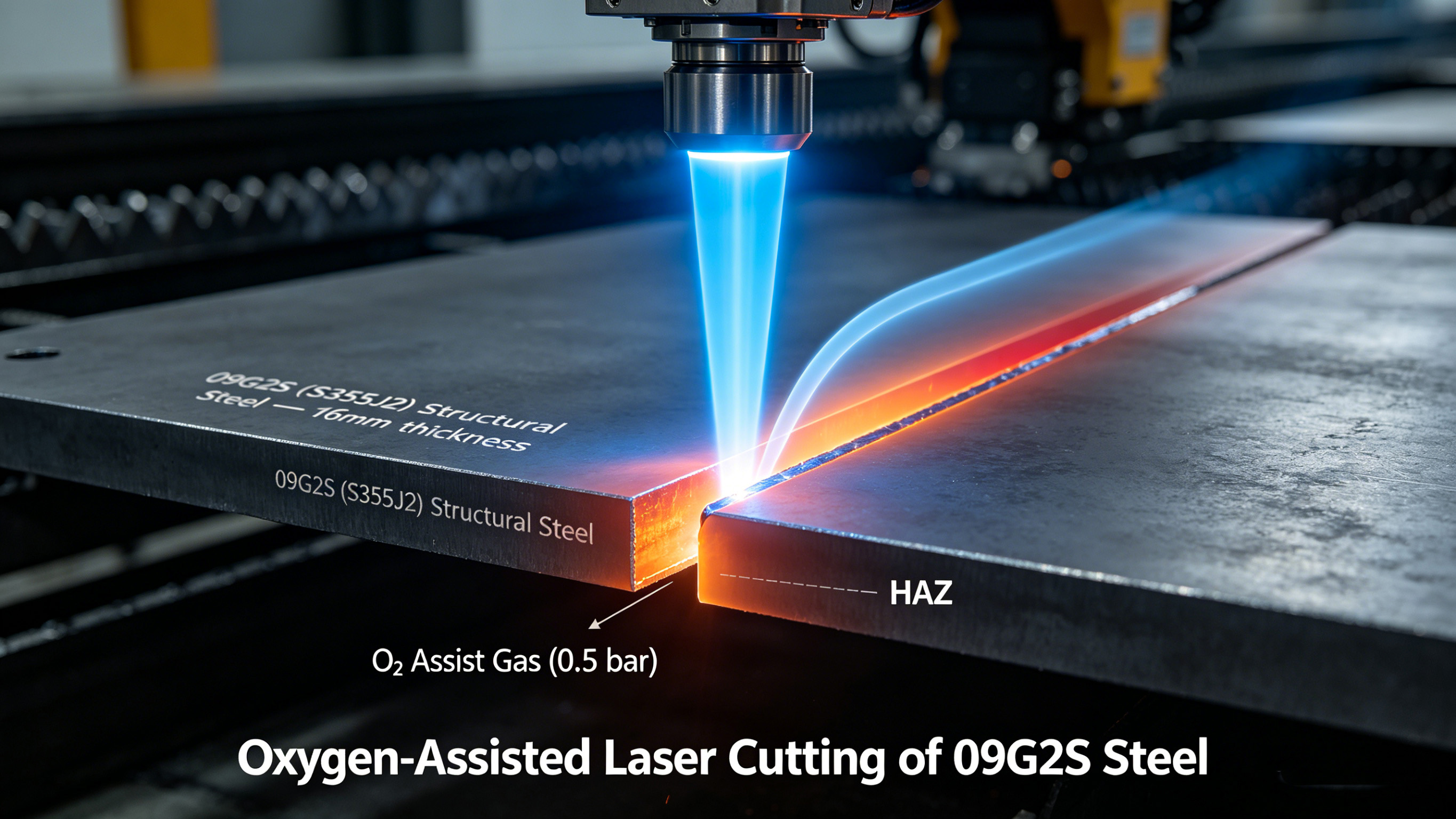
Influence of Cutting Parameters and Assist Gases on the Laser Cutting Quality of 09G2S (S355J2, EN 10025-2) Structural Steel
Related Article