Advanced Semiconductor Packaging – The “Light Knife” Carving of SiC Wafers and TSV
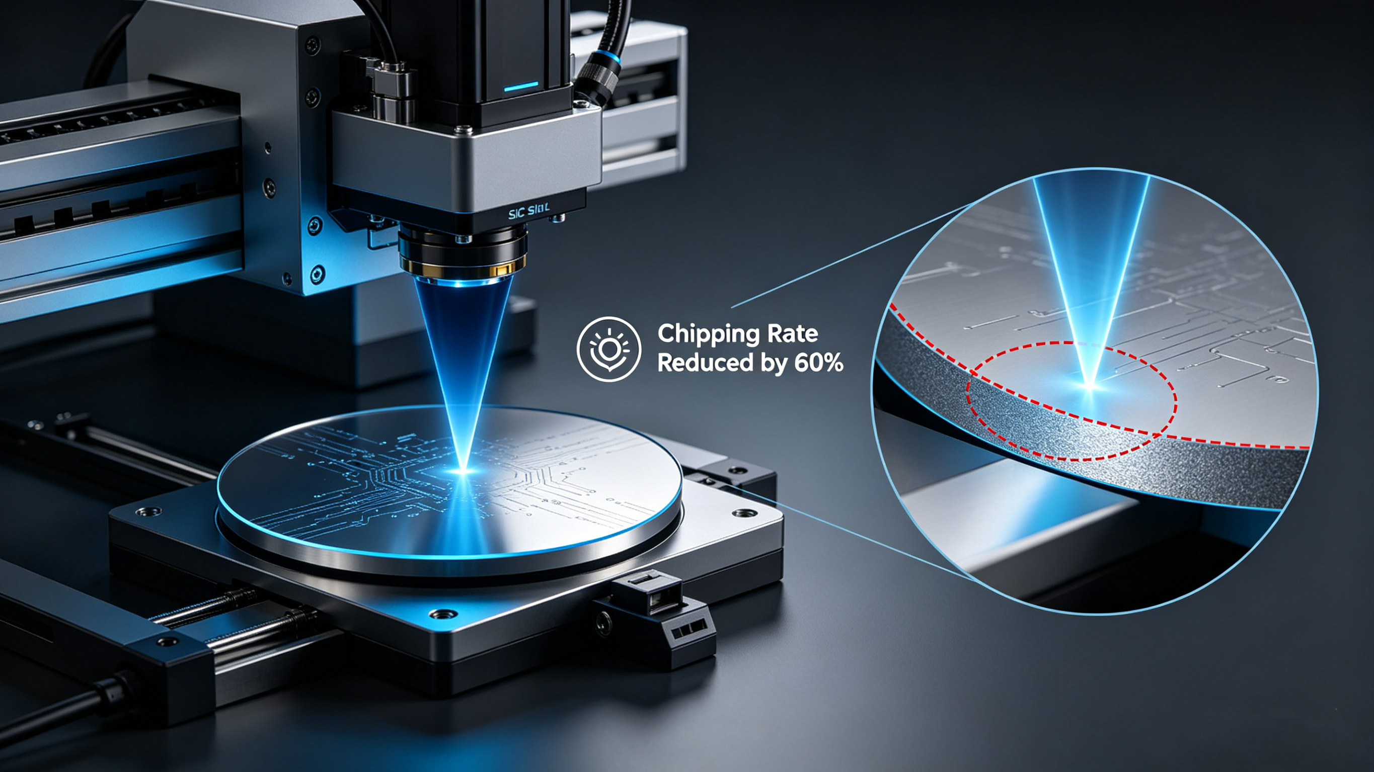
As Moore’s Law slows, advanced packaging has become the engine driving chip performance. By 2026, the compound annual growth rate for ultrafast lasers in semiconductor applications is expected to reach 9.64% – the fastest in the entire laser processing market. Two technologies are leading the charge: laser dicing of silicon carbide (SiC) wafers and through‑silicon via (TSV) drilling with femtosecond lasers. These “light knives” are carving the future of microelectronics.
Industry Background: Packaging Picks Up Where Scaling Leaves Off
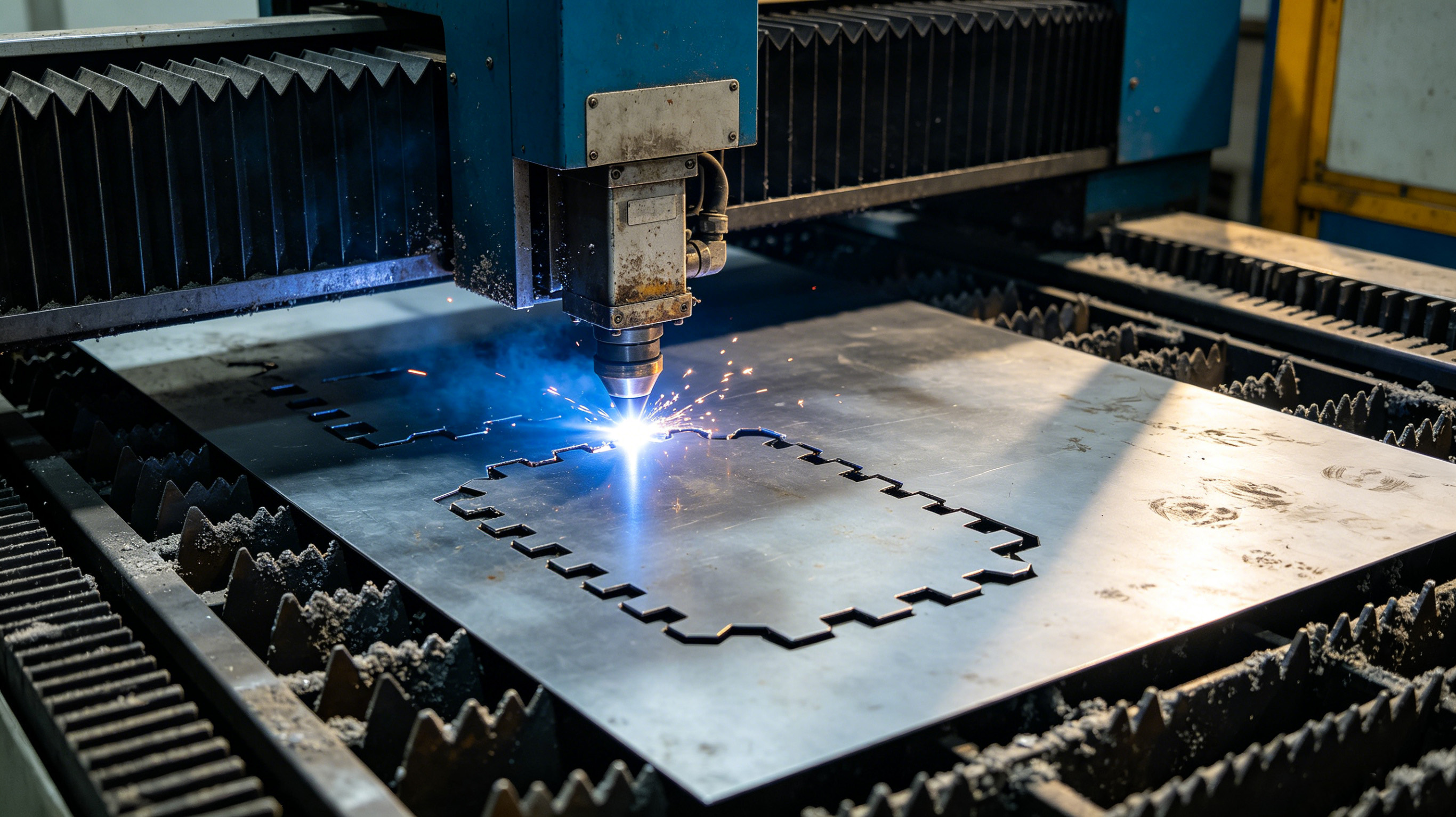
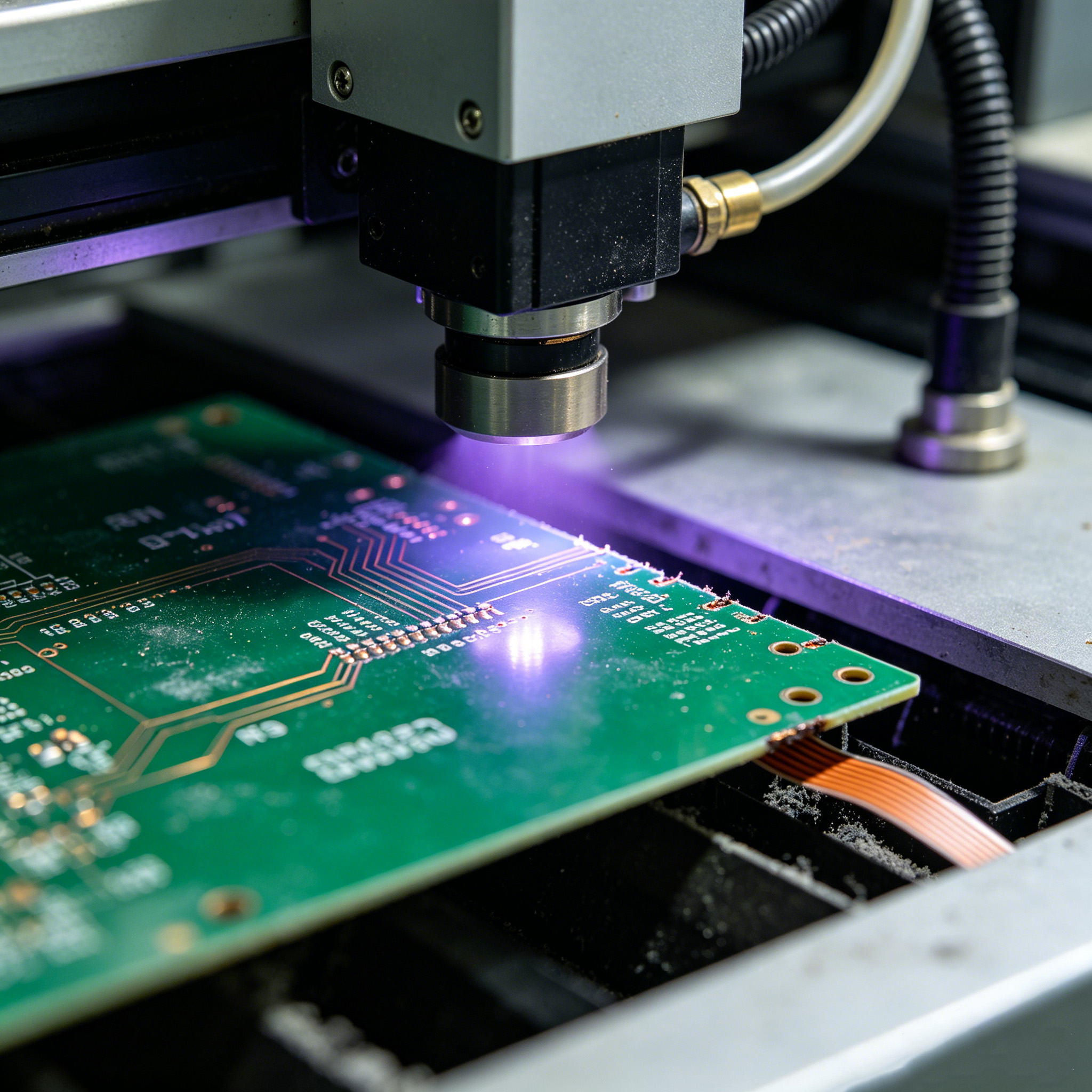
Transistor shrinkage is hitting physical limits. The answer? Stack chips vertically instead of shrinking them horizontally. Advanced packaging – like 2.5D interposers and 3D stacking – demands extreme precision when cutting wide‑bandgap materials and drilling microscopic holes through silicon. Traditional blade dicing causes chipping and cracking. That’s where laser dicing becomes indispensable. It’s non‑contact, produces minimal heat, and handles the toughest substrates.
Core Technology 1: Laser Dicing of SiC Wafers
Silicon carbide is the future of power electronics. But its hardness makes it a nightmare to cut. Mechanical saws leave micro‑cracks and chipping that lower yield. Laser dicing using the stealth (invisible) cutting method focuses the beam inside the wafer, creating a modified layer that allows clean separation. The result: edge chipping reduced by over 60%, thinner die possible, and better heat dissipation. For electric vehicle and 5G power chips, laser dicing has become the standard. More manufacturers are adopting it because it preserves die strength and enables smaller, cooler packages.
Core Technology 2: TSV Drilling with Femtosecond Lasers
Through‑silicon via (TSV) is the backbone of 3D chip stacking. Drilling holes tens of microns wide and hundreds deep through silicon wafers is no easy task. Long‑pulse lasers cause melting, recast, and delamination. The solution: femtosecond laser pulses – trillionths of a second. They ablate material so fast that heat doesn’t have time to spread. This means clean, tapered sidewalls without cracks or debris. TSV drilling with femtosecond lasers enables high‑aspect‑ratio vias for dense interconnects. Memory and logic manufacturers rely on this technology to stack DRAM and logic chips, boosting bandwidth while cutting power consumption.

Policy Support: Local Procurement Gets a Boost
China’s “14th Five‑Year Plan,” along with subsidies in Taiwan, China and South Korea, is accelerating the adoption of domestic laser dicing and TSV drilling equipment. Governments want to reduce reliance on foreign tools. Local laser manufacturers now offer competitive performance at lower prices, making it easier for packaging houses to upgrade. This policy tailwind is driving the shift toward homegrown laser dicing systems.
Case Study: A Memory Manufacturer’s Yield Jump
Consider a leading memory maker that switched from mechanical saws to femtosecond laser dicing for its TSV interposer production. The results: via sidewall roughness dropped by 70%, and inter‑layer dielectric delamination was eliminated. Overall assembly yield climbed by 5 percentage points – a massive gain in a competitive market. By combining laser dicing and TSV drilling in the same process flow, they achieved higher density interconnects with fewer defects. The investment paid back in less than one year.
Future Outlook: Laser Tools Become Core Process Units
As chip architects push toward 2.5D and full 3D packaging, laser dicing and TSV drilling will evolve from optional steps to core process units. Ultrafast lasers will integrate with inline inspection and AI‑driven process control. The “light knife” will carve not just wafers but the entire roadmap for next‑generation semiconductors.

Ready to bring precision laser dicing and TSV drilling to your packaging line? Contact ZGLC Laser for a consultation.
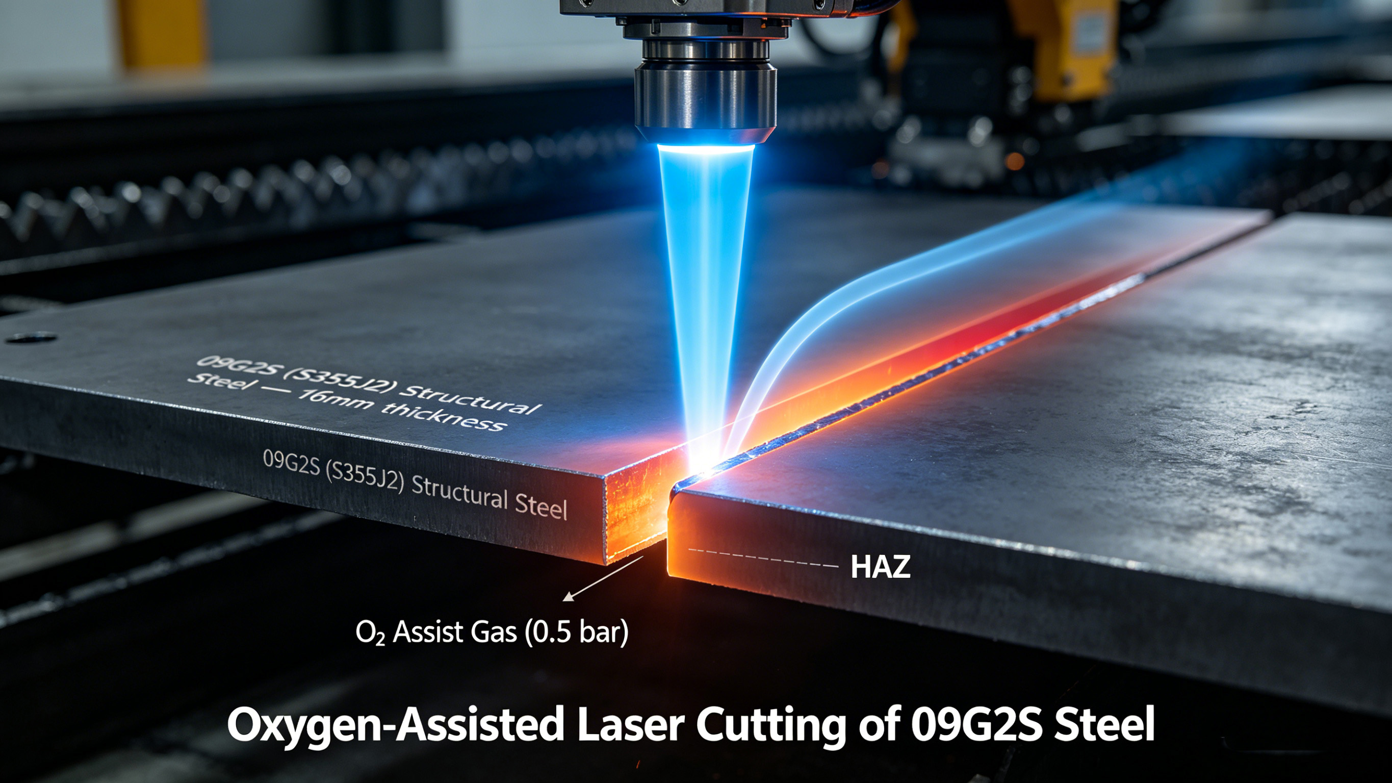
Influence of Cutting Parameters and Assist Gases on the Laser Cutting Quality of 09G2S (S355J2, EN 10025-2) Structural Steel
Mechanical-Assisted QCW Laser Cutting of Carbon Fiber Reinforced Polymer
Related Article